
Waterfall/Matrix
Manufacturer
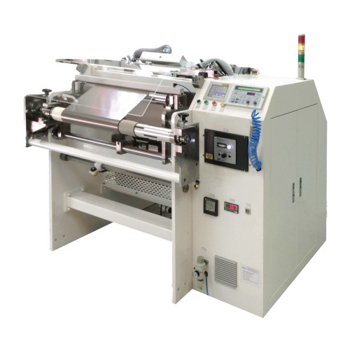
NEMS Tech.Features/Performances
- DBD electrode design: high plasma density.
- Single electrode design
- The reaction gas can be directly used as air (CDA).
- The electrode has a large width.
- The electrode has high expandability and fast processing speed.
- The distance of the sample from the electrode is approximately < 2 mm.
- Can be single or online modular
- Direct plasma
- Can be applied to a variety of sheet, film and coil materials
- Easy to maintain and operate
Performance characteristics
- Only one side of the sample is processed.
- The reaction gas can be directly used as air (CDA).
- Low operating costs
- The effective width of the electrode can be designed according to customer’s requirements, generally 100mm~2000mm (if you want to be wider)
- Generally, the speed that can be processed is 0.5 to 10 m/min. (may be discussed further depending on process requirements)
- The plasma has a high uniformity.
Applications
- Surface cleaning, surface activation, surface wettability, etc. applied to printed circuit boards.
- Surface cleaning, surface activation, surface modification, surface roughening and other functions of polymer materials such as PI, PE and PET.
- Cleaning of glass substrates, ITO glass substrates, etc. of photoelectric displays such as LCD, PDP, and OLED.
- Surface cleaning and surface modification of various components and materials.